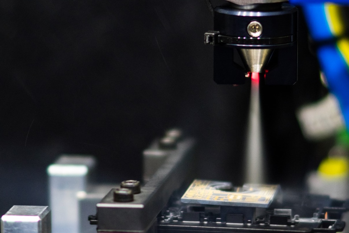
Requirements in electronics
In electronics, particulate and filmic contamination affects downstream processes such as bonding, coating or potting. Clean, defined and prepared surfaces – together with the control of electrostatic charges – are a prerequisite for reliable results.
Production mainly involves small batches, in which every assembly must function reliably. Accordingly, cleaning, surface preparation and electrostatic control are closely interlinked.
Typical components and contamination
From this industry we primarily clean:
- Components: printed circuit boards and assemblies, connectors, sensors, housings, optical electronics as well as chips and bond wires
- Materials: printed circuit boards (FR4), metals such as copper, gold and nickel, plastics, ceramics as well as glass and optics
- Contamination: flux and solder-paste residues, ionic residues, fingerprints, particles and oils
Because many of these residues directly impair downstream processes, the cleanliness target is defined from the respective next step, from bonding to potting.
Suitable processes
Which process fits best depends on the part, the contamination and the batch size: we advise on a technology-neutral basis. For this industry, the following are particularly relevant:
- Electrostatics & ionisation: discharging and cleaning of electrostatically charged surfaces
- CO₂ snow blasting: dry, residue-free cleaning of sensitive assemblies, also for removing solder residues
- Plasma & corona pre-treatment: fine cleaning and surface activation without chemicals
- Wet-chemical cleaning: aqueous or solvent-based cleaning, also of flux residues; frequently with modified alcohols (ZET clean 82 / 82i)
Downstream processes and surface functionalisation
In electronics, cleaning is typically followed by bonding, coating (conformal coating), potting, soldering, adhesive bonding and assembly. Each of these steps requires a defined, prepared surface.
Beyond mere pre-treatment, plasma combined with suitable precursors – frequently silane-based – can be used to apply functional layers, for example hydrophobic coatings or oxidation protection. Plasma also specifically prepares the surface for the subsequent potting of the boards into housings, so that the potting compound adheres reliably.
Electrostatic control and ionised air
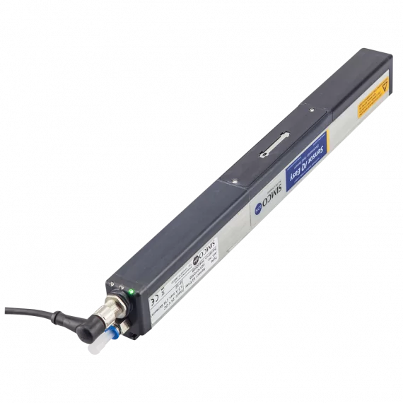
Electrostatic charge is a risk in its own right in electronics manufacturing. With the Simco-Ion range, the charge can be controlled in a targeted manner, for example by supplying machines and manual workstations with neutral ionised air. This prevents particles from being reattracted by the charge and keeps sensitive assemblies protected.
Measurement and quality assurance
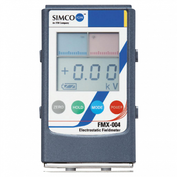
TeSe carries out some of the inspections in-house: checks under a high-resolution microscope with various light sources, contact angle measurement (surface tension) as well as some ESD measurements (Simco-Ion). More advanced tests such as determining ionic cleanliness, residual contamination analyses or scanning electron microscopy (SEM) are predominantly customer-defined processes, which TeSe partly supports.
Application examples
Typical applications from electronics manufacturing at TeSe:
- CO₂ snow specifically eliminates solder residues on sensitive assemblies, dry and residue-free.
- Plasma activates the surface before boards are potted into housings, thereby ensuring adhesion.
- With plasma and silane-based precursors, functional layers are applied: hydrophobic coatings or oxidation protection.
- Neutral ionised air from Simco-Ion keeps machines and manual workstations free of electrostatic charge.
Frequently asked questions
Which electronic parts does TeSe clean? Printed circuit boards and assemblies, connectors, sensors, housings, optical electronics as well as chips and bond wires.
How are flux and solder residues removed? Wet-chemically or dry with CO₂ snow: particularly gentle and residue-free for sensitive assemblies.
Can TeSe control electrostatic charge? Yes. With the Simco-Ion range (including neutral ionised air for machines and manual workstations); ESD measurements are partly possible in-house.
Can functional coatings be applied? Yes. Via plasma with precursors (frequently silane-based) for hydrophobic layers or oxidation protection.
Test the process at TeSe
Whether a process meets your industry’s requirements on your actual part is shown by a trial: 1–2 hours of testing free of charge. In-depth feasibility studies: CHF 1’200 per day, 50% creditable against a machine purchase.
Documents & videos
Datasheets & brochures
Plasma & corona pre-treatment – Ferben
- Ferrarini & Benelli · BrochureEN
Vibration & inline cleaning – Ossberger
CO₂ snow & PowerSnow – ACP
- PowerSnow · BrochureEN
- JetWorker · DatasheetDEEN
- JetWorker High Purity · DatasheetEN
- JetStation · DatasheetDEEN
- JetStation High Purity · DatasheetEN
- JetModule · DatasheetDEEN
- JetModule High Purity · DatasheetEN
- JetCell · DatasheetDEEN
- JetCell High Purity · DatasheetEN
- High Purity Cleaning · BrochureEN
- ACP Systems AG · CertificateDE
- quattroClean CO₂ (Linde) · CertificateEN
Electrostatics / ionisation – Simco-Ion
Static discharge (ionization) 16 datasheets
Ionizing bars
Static charging 8 datasheets
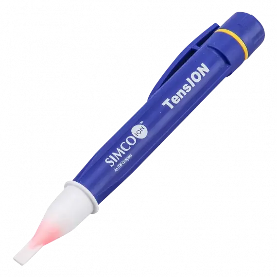
Measurement & control 4 datasheets
Videos
Plasma & corona pre-treatment
CO₂ snow blasting
Electrostatics / ionisation
Process chemistry
Vibration cleaning